I am sorry if you feel I am trying to lead you down a rat-hole, I was just trying to figure out the reference for the eye diagram on
page 11 of traverso_02_0708 shown below:
- You stated the reference is given on page 8 Yagisawa-san which is about 40G compact TOSA with driver
- Mori-san said this is an internal data not published
- Frank said this came from Ref 1 on page 11 Toifl ISSCC 2007, but Ref 1 only implement de-mux and he argues if
you can do a de-mux you can certainly do a mux. Ref 1 when Anrtisu 40G BERT output was applied to the de-mux input had
11 ps error free window, with a realistic transmitter error free window without optics might even get negative!
The authors in this paper are doing leading edge research and I wish they get more support so they can continue their research.
Since I was just asking a technical question on traverso_02_0708 content I am not going to get into a marketing pitch for 4x10G
or against serial 40G!
Thanks,
Ali
Matt Traverso wrote:
Ali,I'm sorry for my error on the reference -- I do resent the implication that my mistake might have been committed in earnest.
Frank,I think Ali was attempting to lead us down a rat-hole here. The key points in our message are:- Serial is the lowest cost in the long term- Serial is technically feasible today- Serial can be made low cost with the first generation of parts thru (a) 1310nm EML, (b) XLMD MSA, (c) minimization of costly RF interconnects (integrated packaging), (d) lack of non-recoverable engineering investment required to build integrated optics for multi-lambda solution, and (e) simpler assembly- Serial can move to CMOS for low power soon- Serial can move to low cost RF interconnects -- more detail to be presented in Korea
Colleagues,I still believe that the IEEE would be best served with a 40GbE 10km SMF objective. I recognize that we seem to be split. I do not want to see the IEEE burdened with a PMD that has such a limited life/application as the 4lambda CWDM proposal. I look forward to our discussion in Korea.
sincerely--matt
On Thu, Sep 4, 2008 at 5:22 PM, Ali Ghiasi <aghiasi@xxxxxxxxxxxx> wrote:
Frank
Ref.1 by Toifl does show an eye diagram similar to traverso_02_0708 except it is the output of the 40Gig Anritsu BERT
to test the de-Mux. Ref .1 did not implement a 40G mux so the eye diagram couldn't have come from this reference unless
someone made an honest mistake.
Thanks,
Ali
Frank Chang wrote:
Mori-san;
I have that Ref.1 by Toifl handy with me, which one of its slides obviously show the similar eye diagram even with same scale. So you may pls kindly re-consider your following comment:
"It was a first time for showing this data in a public place, so there is no paper about this."
Otherwise sound scary to me.
Frank
-----Original Message-----
From: Kazuyuki Mori [mailto:mori.kazuyuki-1@xxxxxxxxxxxxxx] Sent: Wednesday, September 03, 2008 7:50 PM
To: STDS-802-3-HSSG@xxxxxxxxxxxxxxxxx
Subject: Re: [802.3BA] 40G CMOS Ref
Ali-san,
I'm Kazuyuki Mori, Fujitsu Labs. Matt-san may misunderstand for your question.
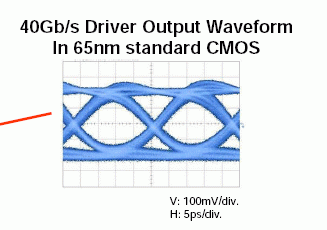
The eye diagram of page 11 in traverse_02_0708 is our test chip result using 65nm standard CMOS. It was a first time for showing this data in a public place, so there is no paper about this. The circuit architecture is almost the same as our 90nm design shown in ISSCC2005 8.2.
Kazuyuki Mori
----- Original Message ----- From: "Frank Chang" <ychang@xxxxxxxxxxx>
To: <STDS-802-3-HSSG@xxxxxxxxxxxxxxxxx>
Sent: Thursday, September 04, 2008 10:16 AM
Subject: Re: [802.3BA] 40G CMOS Ref
Ali;
I have interest to understand this as well. I feel the laser driver doesnot have to be CMOS such as in 10G for better performance.
I think what in Matt's slides actually talking about the high-speed driver portion of the CDR, which indicated in its Ref.1 of pg.11 by Toifl. Here is what I can find from google search for this Ref.
ISSCC2007
12.3 A 72mW 0.03mm2 Inductorless 40Gb/s CDR in 65nm SOI CMOS
9:30 AM
T. Toifl, C. Menolfi, P. Buchmann, C. Hagleitner, M. Kossel, T. Morf, J. Weiss,
M. Schmatz
IBM, Rueschlikon, Switzerland
A quarter-rate CDR circuit is based on a dual-loop approach where sampling phases are
generated by a phase-programmable PLL that is controlled by a digital DLL.
Implemented in 65nm SOI CMOS, the chip occupies 0.03mm2 and consumes
1.8mW/Gb/s. Measurements confirm 40Gb/s operation with a BER <10-12 at a maximum
frequency-offset of 400ppm. The phase relation between data and edge samples can be
programmed within ±0.1UI.
________________________________
From: Ali Ghiasi [mailto:aghiasi@xxxxxxxxxxxx]
Sent: Wednesday, September 03, 2008 4:53 PM
To: STDS-802-3-HSSG@xxxxxxxxxxxxxxxxx
Subject: Re: [802.3BA] 40G CMOS Ref
Matt
I looked at reference on page 8 Yagisawa-san's paper title "Compact 40-Gbit/s Electroabsorption Monolithically
Integrated DFB Laser (EML) Module with a Driver IC for Very Short Reach Application". The EML driver
IC is not described in this paper, but to drive an EML I expect the driver IC to be either in InP or SiGe.
Based on this driver data how did you arrive at the following statement on page 11 "40 Gb/s Driver Output Waveform In
65 nm Standard CMOS"? You are using InP or SiGe driver performance as proof that 40Gb/s is possible in
65 nm CMOS!
Thanks,
Ali
Matt Traverso wrote:
Ali,
The reference for page 11 is the same as the reference on page 8 -- Yagisawa-san's paper. My apologies that this was not clearer in the presentation.
--matt
On Wed, Sep 3, 2008 at 3:14 PM, Ali Ghiasi <aghiasi@xxxxxxxxxxxx> wrote:
Mat
I was reviewing your presentation from Denver traverso_02_0708. On page 11 you show an eye diagram
under sub-title "40Gb/s Driver Output Waveform in 65 nm standard CMOS", I assumed the reference for
this eye diagram was included in one of the 3 reference listed on this page. Can you please provide the
supporting material for reference eye diagram.
Thanks,
Ali